In today’s electronics-driven world, nearly every device—whether it’s a smartwatch, home appliance, industrial controller, or medical monitoring system—relies on high-quality PCB assembly (PCBA). As products become more compact and more intelligent, the expectations for PCB quality, speed, and reliability have risen dramatically.
Understanding the full PCBA manufacturing process helps engineers, sourcing teams, and product developers make better decisions, avoid production risks, and optimize costs. This guide breaks down every major step involved in turning a bare PCB into a fully assembled, functional electronic board.
1. What Is PCBA?
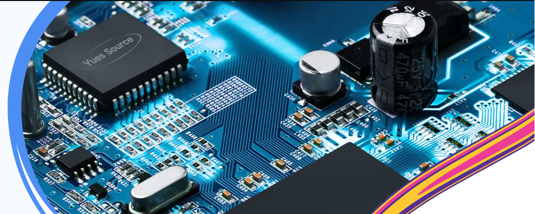
PCBA (Printed Circuit Board Assembly) refers to the full process of mounting and soldering electronic components—both SMT and through-hole—onto a bare PCB to create a working electronic circuit.
PCBA includes:
THT (through-hole) insertion
Wave soldering or selective soldering
Reflow soldering
Inspection (AOI, X-ray, ICT, FCT)
Programming, testing & final assembly
In modern electronics, PCBA is one of the most important steps in bringing a product from concept to reality.
2. PCBA vs PCB: What’s the Difference?
|
Term |
Meaning |
Description |
|
PCB |
Printed Circuit Board |
Bare board without components |
|
PCBA |
PCB Assembly |
Fully assembled and functional board |
A PCB is the “skeleton,” while PCBA represents the “complete body” with electronic components.
3. Overview of the PCBA Manufacturing Workflow
A standard PCBA line includes:
DFM Review (Design for Manufacturability)
PCB fabrication
Incoming materials inspection (IQC)
Solder paste printing
SMT component placement
Reflow soldering
AOI inspection
THT insertion (if needed)
Wave soldering / selective soldering
X-ray inspection (BGA/QFN)
ICT/FCT testing
Cleaning, coating & packaging
Below, we break down each step in detail.
4. Step-by-Step PCBA Manufacturing Process
Step 1: DFM Analysis (Design for Manufacturability)
Before production begins, experienced engineers evaluate the customer’s Gerber files, BOM, and assembly drawings.
Key checks include:
Pad size and spacing
Solder mask definition
BGA escape routing
Component clearance
Thermal relief design
PCB material suitability
A strong DFM review prevents:
open circuits
shorts
solder bridging
tombstoning
misalignment
warping during reflow
Ample Chip performs mandatory DFM checks for every new PCBA project to ensure stable mass production.
Step 2: PCB Fabrication (One-Stop or Customer-Supplied)
If the manufacturer provides one-stop PCBA service, PCB fabrication is included.
PCB manufacturing includes:
material selection (FR-4, CEM-1, Rogers, high-Tg, aluminum substrates)
copper lamination
drilling & plating
solder mask printing
silkscreen
surface finishing: HASL, ENIG, OSP, immersion silver, ENEPIG
electrical testing (E-test)
High-quality PCB fabrication ensures:
stable impedance
consistent copper thickness
reliable solderability
minimal warpage
Ample Chip supports HDI, high-layer PCBs, flexible boards, and rigid-flex structures.
Step 3: Material Procurement & IQC (Incoming Quality Control)
PCBA quality depends heavily on reliable components.
This step verifies all purchased materials:
Original chips & ICs
Passive components (R/C/L)
Connectors
Sensors
Batteries & modules
IQC testing includes:
visual inspection
solderability tests
packaging integrity
ESD compliance
lot traceability
A strong supply chain helps avoid counterfeit or refurbished parts—one of the biggest risks in PCBA manufacturing.
Step 4: Solder Paste Printing
A stainless stencil is used to apply solder paste to exposed copper pads.
Key factors:
stencil thickness
solder paste type (lead-free, SAC305, fine-pitch)
squeegee pressure
printing speed
Poor solder paste printing accounts for 60–70% of SMT defects, making SPI inspection (next step) essential.
Step 5: SPI (Solder Paste Inspection)
3D SPI verifies:
height
volume
position accuracy
bridging
insufficient solder
If errors are detected, the SMT line automatically alerts technicians.
Step 6: High-Speed SMT Component Placement
Pick-and-place machines mount components such as:
resistors & capacitors
ICs
BGA, QFN, LGA
oscillators
MOSFETs, drivers
connectors
sensors & modules
Top-level SMT lines support:
01005 / 0201 components
0.25–0.4 mm pitch ICs
multi-zone reflow ovens
high-precision placement cameras
Ample Chip handles both prototypes and mass production in the same high-quality assembly environment.
Step 7: Reflow Soldering
The PCB enters a temperature-controlled reflow oven, where the solder paste melts and forms electrical connections.
A standard lead-free reflow profile includes:
Preheat
Soak
Liquidus (reflow zone)
Cooling
Improper reflow can cause:
tombstoning
solder balls
cold joints
excessive voids
Experienced technicians optimize temperature curves based on board size, copper weight, and component density.
Step 8: AOI Inspection
AOI scans every component to detect:
missing parts
misalignment
polarity errors
solder defects
bridging
High-quality AOI catches over 95% of common SMT issues.
Step 9: THT Assembly (Manual or Automated)
Some components still require through-hole mounting, such as:
connectors
transformers
electromechanical parts
power inductors
relays
large capacitors
Insertion can be:
fully manual
semi-automated
selective for high-mix boards
Step 10: Wave Soldering / Selective Soldering
For boards with many THT parts, wave soldering is used.
Selective soldering is preferred for mixed-technology boards to avoid damaging SMT components.
Step 11: X-Ray Inspection (for BGA / QFN)
Invisible solder joints under chips require X-ray imaging.
X-ray checks:
void ratio
bridging under BGA balls
collapsed balls
open circuits
This is critical for automotive, medical, and high-reliability electronics.
Step 12: ICT, FCT and Programming
To ensure the assembled PCB works perfectly:
ICT (In-Circuit Test)
Tests electrical values:
resistance
capacitance
logic states
short/open circuits
FCT (Functional Test)
Simulates real working conditions.
MCU programming
Microcontrollers and memory chips are programmed with firmware before final testing.
Step 13: PCBA Cleaning (Optional)
Removes:
flux residue
ionic contaminants
solder balls
dust and oils
Critical for medical, aerospace, and automotive boards.
Step 14: Conformal Coating & Final Assembly
Coating protects the PCBA from:
moisture
corrosion
chemicals
dust
vibration
Methods include:
spray coating
dip coating
selective coating
Final step: packaging and shipment.
5. Why High-Quality PCBA Matters
A poor-quality assembly can cause:
overheating
unstable operation
early product failures
warranty claims
safety hazards
EMC interference
Reliable PCBA ensures:
longer product life
stable performance
fewer returns and repairs
faster time-to-market
6. Why Choose Ample Chip for PCBA Manufacturing?
Ample Chip provides one-stop PCBA service, including:
PCB fabrication
SMT assembly
THT assembly
Component sourcing
Prototyping in as fast as 24 hours
Mass production
Strict QC (SPI, AOI, X-ray, FCT)
Capabilities include:
Minimum component size: 01005 / 0201
Fine-pitch ICs: 0.25 mm
BGA assembly & X-ray inspection
High-speed SMT lines
Global component sourcing with traceability
This combination ensures stable, cost-effective, and on-time delivery for all PCBA needs.
7. Conclusion
The PCBA manufacturing process may seem complex, but each step plays an essential role in ensuring performance, reliability, and longevity. From DFM checks to final functional testing, attention to detail determines whether your product succeeds in the market.
With advanced SMT equipment, strong supply chain resources, and fast prototyping services, Ample Chip provides manufacturers worldwide with a dependable, high-quality, one-stop PCBA solution.
Related News
What Is SMT Assembly? A Complete Guide
Why Choose Ample Chip for PCB-SMT Support
One-Stop Solution for PCBA: From Component Sourcing to Assembly
PCBA vs PCB vs SMT: What’s the Difference?
The Complete PCBA Manufacturing Process Explained