Ideal for PCBA beginners, engineers, sourcing teams, and procurement managers
Surface Mount Technology (SMT) has become the foundation of modern electronics manufacturing. From smartphones and IoT sensors to industrial controllers and medical devices, nearly every electronic product today relies on SMT assembly for its compact size, high performance, and manufacturing efficiency.
If you are new to electronics production, understanding SMT assembly will help you make better decisions when selecting manufacturers, controlling product quality, and accelerating your development cycle.
This guide explains what SMT is, how the SMT process works, why it matters, and how companies like Ample Chip deliver high-speed and high-reliability SMT services.
1. What Is SMT Assembly?
SMT Assembly (Surface Mount Technology Assembly) is the process of placing electronic components directly onto the surface of a PCB (Printed Circuit Board). Instead of inserting leads into drilled holes—like in traditional THT (Through-Hole Technology)—SMT relies on solder paste and reflow soldering to secure components.
Key Characteristics of SMT:
No holes required → allows for dense component placement
Supports very small components (e.g., 01005, 0201 size)
Enables high-speed, automated production
Reduces cost and improves manufacturing efficiency
Because SMT creates lighter, smaller, and more complex PCB assemblies, it has become the global standard for electronics production.
2. Why SMT Replaced Traditional Through-Hole Assembly
While THT is still used for special components (connectors, transformers, relays), SMT dominates for three major reasons:
a. Miniaturization
Modern electronics demand extremely small components. SMT supports micro-sized parts like resistors, capacitors, ICs, BGAs, and QFNs.
b. Higher Circuit Density
No drilling means more space for routing, enabling multi-layer and HDI PCB designs.
c. Faster & Cheaper Production
SMT pick-and-place machines can mount tens of thousands of components per minute, dramatically reducing labor and assembly costs.
This is why nearly all compact consumer products rely heavily on SMT.
3. The SMT Assembly Process: Step-by-Step Explained
Below is the complete SMT manufacturing workflow used in professional PCBA factories like Ample Chip.
Step 1: Solder Paste Printing
Using a stainless-steel stencil, solder paste is printed onto the PCB pads with high precision.
Key requirements:
Proper stencil thickness (typically 100–150 μm)
Uniform paste distribution
Clean edges to prevent solder bridging
Step 2: SPI (Solder Paste Inspection)
A 3D SPI machine checks:
paste height
paste width
volume
alignment
If solder paste deposit is incorrect, the SMT line will stop automatically to avoid defects downstream.
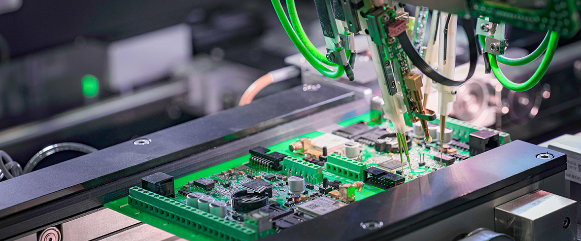
Step 3: High-Speed SMT Component Placement
Pick-and-place machines place components onto the PCB with speeds up to 50,000–80,000 CPH (components per hour).
Common SMT components:
Resistive & capacitive chips (R/C)
ICs and microcontrollers
QFP / QFN
BGA / LGA
Sensors, oscillators, LEDs
Ample Chip's lines support:
01005 ultra-small components
Fine-pitch ICs
High mix / low volume production
Large-scale mass production
Step 4: Reflow Soldering
Boards then enter a multi-zone reflow oven, where solder melts and bonds components to the PCB.
A proper reflow profile includes:
Preheat
Soak
Reflow (liquidus)
Cooling
Any deviation may cause:
tombstoning
cold solder joints
solder voids
component misalignment
Step 5: AOI Inspection
Automated Optical Inspection checks:
missing parts
wrong polarity
solder bridges
insufficient solder
incorrect placement
High-quality PCBA manufacturers use AOI after every SMT line.
Step 6: X-Ray Inspection (for BGA / QFN)
Hidden solder joints under BGAs cannot be inspected visually.
X-ray detects:
solder voids
bridging under the chip
insufficient solder balls
Step 7: Rework & Manual Inspection
Complex components may require fine soldering by certified technicians.
Step 8: Functional Testing (FCT)
To ensure the PCBA works as intended, FCT simulates actual working conditions:
power on testing
signal integrity testing
program burning
ICT / flying probe testing
4. Advantages of SMT Assembly
a. Smaller Product Size
Critical for IoT devices, wearables, medical sensors, smartphones.
b. Lower Manufacturing Cost
Less drilling, faster automation, fewer manual steps.
c. Better Electrical Performance
Shorter interconnects → lower inductance → improved signal integrity.
d. Higher Reliability
Reflow soldering creates stronger connections compared to manual solder.
e. High-Speed Production
Ideal for large-volume electronics manufacturing.
5. Common SMT Defects and How Manufacturers Avoid Them
1. Tombstoning
Caused by uneven solder paste or temperature imbalance.
2. Bridging
Pads too close, excessive solder.
3. Insufficient Solder
Stencil thickness mismatch.
4. Misalignment
Caused by inaccurate placement or improper PCB design.
5. BGA Voids
Fixed with controlled reflow profiles and X-ray inspection.
Professional factories like Ample Chip minimize defects through:
DFM checks
SPI + AOI
X-ray for hidden joints
Strict quality control
6. SMT Assembly Applications Across Industries
SMT is essential for:
Consumer Electronics
Smartphones, tablets, cameras, audio devices
Industrial Electronics
PLC, control boards, industrial sensors
Medical Devices
ECG monitors, wearable medical sensors, diagnostic equipment
Automotive Electronics
ADAS, EV battery management, dashboards, control units
Telecom & Networking
Routers, base stations, antennas, IoT gateways
LED Lighting
Drivers, COB modules, LED panels
7. Choosing the Right SMT Assembly Manufacturer
When selecting an SMT partner, check for:
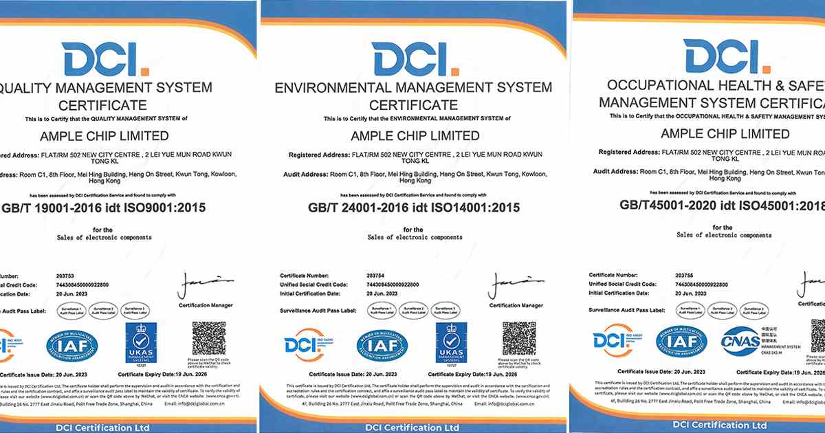
Certification (ISO 9001, ISO 13485, IATF 16949)
Equipment (high-speed SMT machines, reflow with precise control)
Testing capabilities (AOI, X-ray, FCT)
Component sourcing ability
Lead time for prototypes & mass production
Ample Chip offers:
High-speed SMT assembly
24-hour quick-turn PCBA prototyping
One-stop service including BOM sourcing, PCB fabrication, and testing
Small-batch and large-batch production
8. Final Thoughts
SMT assembly is the backbone of modern electronics manufacturing.
Whether you are building an IoT device, industrial controller, or medical-grade equipment, choosing the right SMT partner ensures faster production, lower costs, and higher reliability.
With advanced SMT lines, strict quality control, and rapid prototyping capabilities, Ample Chip provides a complete one-stop solution for all PCBA manufacturing needs.
Related News
What Is SMT Assembly? A Complete Guide
Why Choose Ample Chip for PCB-SMT Support
One-Stop Solution for PCBA: From Component Sourcing to Assembly
PCBA vs PCB vs SMT: What’s the Difference?
The Complete PCBA Manufacturing Process Explained